pcbshow.net
乐可佳苑酒店(北京)有限公司
约"惠"在酒店,女人节尊享3.8折起酒店,约"惠"在酒店,女人节尊享38折起酒店,约"惠"在酒店,女人节尊享3.8折起酒店.
 pcbsi-ph.com
PCBSI
Prudential Customs Brokerage Services. Arrastre and Stevedoring Branches. Prudential Customs Brokerage Services, Inc. (PCBSI) is a corporation, incorporated under Philippine Laws, registered with the Securities and Exchange Commission (SEC). The company has now grown to nine (9) branches, three (3) RORO ports and its affiliated companies with offices and branches nationwide. Because we value our customers the most, we will do our best to meet our customers' current and future needs with integrity, honest...
 pcbsi.com
av天堂网
讨论交流信号完整性SI,电源完整性PI,电磁兼容EMC 理论/建模/仿真/EDA工具. 2015-6-16 15:00 zx sha. 2015-6-30 11:15 QQ 9E6CB8. GMT 8, 2015-8-12 11:45 , Processed in 0.033036 second(s), 10 queries , Gzip On. 积分 0, 距离下一级还需 积分.
 pcbsi.com.ph
Prudential Customs Brokerage Services, Inc.
Prudential Customs Brokerage Services, Inc. 7603 Dela Rosa Centre, Dela Rosa St., Pio Del Pilar. Makati City, Philippines 1230. Phone: 63(2)812-6085 to 88 / Fax: 63(2)812-9884. Email: admin@pcbsi.com.ph. Welcome to PCBSI Website. PCBSI started out in the business of customs brokerage. The business expanded when the company represented the business interests of foreign shipping companies, importers/exporters and manufacturers here in the Philippines. The company's major services are cargo handling...We va...
 pcbsig.com
pcb设计_pcb抄板_程序开发_电路设计图_单片机开发板_pic/avr单片机_集成电路板_at89s52最小系统_allegro_滤波器设计_软件工具_Pcb信息人才网_STM32_东远电路设计公司
北京市 上海 广州 深圳 天津. 苏州市 重庆 成都 杭州 无锡. 武汉市 青岛 佛山 南京 大连. 宁波市 沈阳 长沙 唐山 烟台. 哈尔滨 郑州 东莞 济南 泉州. 石家庄 南通 长春 合肥 西安. 福州市 大庆 徐州 常州 潍坊. 鄂尔多斯市 温州 淄博 绍兴. 济宁市 盐城 洛阳 临沂 嘉兴. 包头市 东营 扬州 南昌 台州. 沧州市 邯郸 厦门 昆明 鞍山. 保定市 泰州 金华 镇江 吉林. 南阳市 中山 南宁 宜昌 襄阳. 呼和浩特市 威海 惠州 太原. 德州市 岳阳 江门 聊城 常德. This DXF file is newer than the formats supported by PADS Layout Export/Import问题解决方法. Keil出现Deprecated declaration Led GPIO Configuration - give arg types警告信息原因及解决方法. 高速PCB设计 EMC 电磁兼容 设计 EDA工具 信号完整性分析 测试测量技术 SMT加工 电路设计 关于知识产权.
 pcbsignalintegrity.blogspot.com
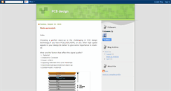
PCB design
Sunday, August 15, 2010. Choosing a perfect stack-up is the challenging in PCB design technology.If you have PCIe,LVDS,HDMI, or any other high speed signals in your design,its better to give some importance to stack-up. What are the factors that affect the signal quality? 4Spacing between the core materials. Its a good practice to avoid solder-mask on the high speed traces. solder-mask is also a dielectric material which will play some role.Having air medium for high speed trace is advisable. Schematics ...
 pcbsinc.net
PC Business Solutions
 pcbsingulation.com
pcb depaneling, singulation of v-scored, tab-routed circuit boards
Subscribe to our Email Newsletter. PCB Depaneling for Tab-Routed and V-Scored Circuit Boards. Pioneer Dietecs offers a complete line of depaneling systems. For close tolerance singulating of v-scored and tab-routed printed circuit boards. The Pioneer system is a press-based, stress-free system. That includes both dies and presses. Pioneer Dietecs tooling offers the same accuracy as hard tooling for a fraction of the cost. Typical PCB Depaneling Designs. Download pdf of 6 design tips for PCB depaneling.
 pcbsino.com
PCB Manufacturer China|Flexible/Rigid-flex/MCPCB/Rogers,Quote online,Fast PCB
Chinese Flexible PCB ,Rigid-flex PCB,MCPCB, Manufacturer/Vendor/supplier, Quote online. PCB Contract manufacturer, PCB Fabrication,Buried and Blind Via PCB Fast Prototype;. PCB maker Outsourcing,Aluminum Al metal core PCB, Low cost,Shenzhen,China/USA/UK/India. PCB Manufacturer Shenzhen, China,Quote online,Flexible/Rigid-flex/MCPCB/Rogers/Multilayer PCB,Fast Prototype Manufacturing,Low cost Express PCB Supplier/vendor. Gold Plating PCB,Immersion Gold/Silver surface, HASL surface.Heavy Copper PCB,. Custome...
 pcbsino.org
PCB Assembly Service China|Electronic Manufacturing EMS
PCB Assembly Services in China, Electronic Manufacturing Factory/Company, EMS/OEM SMT House,. PCB Prototyping&Mass production Factory, PCB Assembly Shenzhen,Electronic Contract Manufacturing,. Prototype/ Turnkey Solution, Electronic Product Assembly Services, USA/UK/India/South Africa. Box Build casing Assembly. China PCB Assembly Services, PCB Prototype Manufacturing, Electronic SMT House, EMS/OEM Production, Turnkey Solution, Contract PCBA Company Outsourcing. Electronic product Contract Manufacturing.
 pcbsistemas.com
PCBTelecom » Comunicaciones a su medida
Http:/ courtesy.nominalia.com/index.html.